

Circuit Design Guidelines
Compatible Gerber File Extensions
A Gerber export produces numerous files, the V-One software uses the file extension to determine what board layer the file belongs to.
Layer | Extensions |
Top | gtl, gbr, top, cmp, art |
Bottom | gbl, bottom, sol, art |
Solder Paste | gtp, gbp, sts, gbr, art |
Drill | txt, drl, drill |
If your CAD tool uses a different file extension for Gerber formatted files, you can simply rename your output file to an appropriate extension and load it.
Pro tip: If you load a *.GBL or *.GBP file, the software will automatically mirror it in the X axis.
Design Rules
Keep the following in mind when designing circuits that will be printed by the V-One:
Minimum 8 mil (0.2mm) trace width and trace spacing - however, we recommend 10 mil for new users.
Minimum 0.65mm pin pitch for SMT IC packages (0.5 mm for solder paste).
Minimum 0603 passive size (0402 for solder paste).
Use hatched planes rather than solid planes. This conserves ink and reduces print time.
Use standard packages and pad shapes. Custom pad shapes can lead to processing errors.
Minimum circuit size is 1 x 1 mm
Keep in mind: The Voltera V-One will try to print any feature that is included in the loaded Gerber file. For this reason, we do not recommend including board outlines, dimensions, silkscreen, or other layers in the copper layers.
Conductivity Considerations
It's best to check the Data sheet of the material you have for its resistivity values. As an example, Conductor 3 has a bulk resistivity of 1.27E-4 Ohm and a sheet resistance of 2.4 mOhm/sq (with a 15 μm film thickness). Some general considerations for silver ink:
Silver conductive ink is approximately one order of magnitude less conductive than copper.
Wider traces will have lower resistance and can handle more current.
The current capacity of the ink depends on the maximum temperature of your application.
The ink thickness is configurable, which can change the sheet resistance.
Pours, Planes, and Polygons
Hatch Planes
If your design requires power or ground planes or other sections of solid infill, we highly recommend that you change the fill to a hatch plane. This will conserve ink and print much faster, with negligible difference in performance for most applications.
Set the Width setting to less than 14 mil (0.014"). If you have adjusted the Pass Spacing parameter in the V-One software, reduce the Width to less than 2x the pass spacing.
Set the Isolate setting to 16 mil or more. Isolate determines how much space there is between the polygon and different, non-connected features.
Set the Spacing setting as large as is reasonable. Denser hatches will have lower resistance, but will also take longer to print.
Solid Pours and Polygons in EAGLE CAD
If you absolutely require a solid in-fill, it's important to know that solid in-fill features like planes, pours, and polygons will be exported differently, depending on the CAD program!
Some, like EAGLE, will export pours and polygons as a series of parallel lines
Others, like Altium, export pours and polygons as contours (a string of points that define a polygon)
When processing EAGLE files, it is difficult to determine if we are parsing a pour, or lines that just happen to be parallel. The problem occurs when the spacing between the parallel lines is too small to print - the end result would be a section that is flooded with ink!
To print these properly, adjust the polygon settings in EAGLE before exporting the Gerber files:
Set the Width setting to 16 mil (0.016")
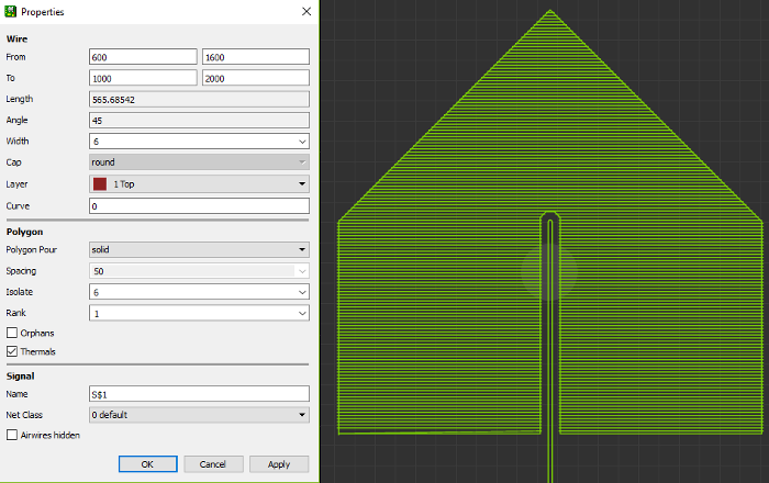
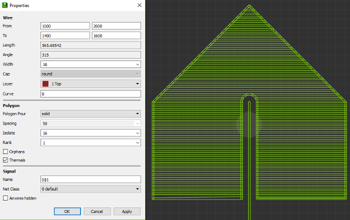
Set the Isolate setting to 16 mil or more. Isolate determines how much space there is between the polygon and separate non-connected features. For illustration purposes, compare the two images below:
The first image shows a polygon with 6 mil width and isolate.
The second image below shows the same polygon with 16 mil width and isolate.
Last updated